
Renovation began this week in NTW’s Metalorganic Chemical Vapor Deposition (MOCVD) Lab located in Room 200 to prepare for the installation of a new dual-chamber Nitride MOCVD system which was moved into NTW on September 21, 2017. The Agilis MOCVD system manufactured by Agnitron has been enabled by Professor Hongping Zhao (ECE), a Materials and Manufacturing for Sustainability (M&Ms) Discovery …
Energy Storage Lab Adds 32 Cubic Foot Environmental Test Chamber
NTW’s new Energy Storage Lab (located in Room 106 on the first floor) has started its’ buildout with the installation of a large environmental testing chamber (ENV01). While the remainder of the lab will continue to be facilitized over the coming months under the direction of Professors Jung Hyun Kim and Vicky Doan-Nguyen, the environmental chamber is now available for …
NTW Lab Management System Adds Cleanroom Displays
NTW’s Lab Management System (or “swipe” system) has been upgraded to include 43″ display monitors in each bay of the cleanroom. The display in each bay contains some schedule details (current, previous and next user) for each tool located in that bay as well as a list of tools currently in use throughout the rest of the cleanroom. Some displays …
MICA Lab Adds Low Temperature Probe Station
NTW’s Mid-Infrared Characterization and Application (MICA) lab (located in Room 117) continues its buildout with the addition of a Lakeshore CRX6.5k cryogenic probe station (tool code PRB07) to provide low temperature device probing capability. Cooled by a closed cycle helium compressor the probe station supports measurements between 6.5K and 350K. The system is configured with four Triax probe arms and …
Device Packing Capability Added with Flip Chip Bonder Installation
Nanotech West Labs has recently expanded its device packaging capabilities with the installation of a SET FC150 (tool code BND04) “flip chip” bonder. Designed to enable precision aligned chip or die bonding, the machine is configured with a low-contact force (up to 4N) solder reflow arm (SRA) with 2″ chucks as well as a laser leveling system. A split field …
New Lapping and Polishing Capabilities at Nanotech West
Nanotech West now offers the capability to thin samples down and polish samples smooth using the new PM4 lapper and PM5 polisher. The last polishing step offers a contamination-free colloidal silica environment for nanometer-scale final roughness. These processes would be excellent for preparing samples for bonding, eliminating damage after ion implantation, damascene-style metal patterning, optical surface preparations, creating thin layers …
Nanotech West Obtains Optical Profilometer
Nanotech West announces the availability of a Zeta-20 optical profilometer, located in Bay 3 of the cleanroom. The tool (tool code INS09) is capable of the 3D imaging of surfaces with a z resolution of ~15 nm, as well as serving as an excellent optical microscope. Its purchase was enabled by the Ohio Sensor and Semiconductor Innovation Platform (OSSIP) program, …
Nanotech West and NanoSystems Labs Announce Annual Retraining Schedule
Nanotech West and the NanoSystems Labs are announcing their Annual Safety Retraining Program (ASRP) schedule. The sessions will start the third week of May, immediately after IMR Materials Week. Twenty-three sessions are currently scheduled, both in campus and at Nanotech West. All Columbus-area users are required to attend a session. As before: If in the past you have attended a …
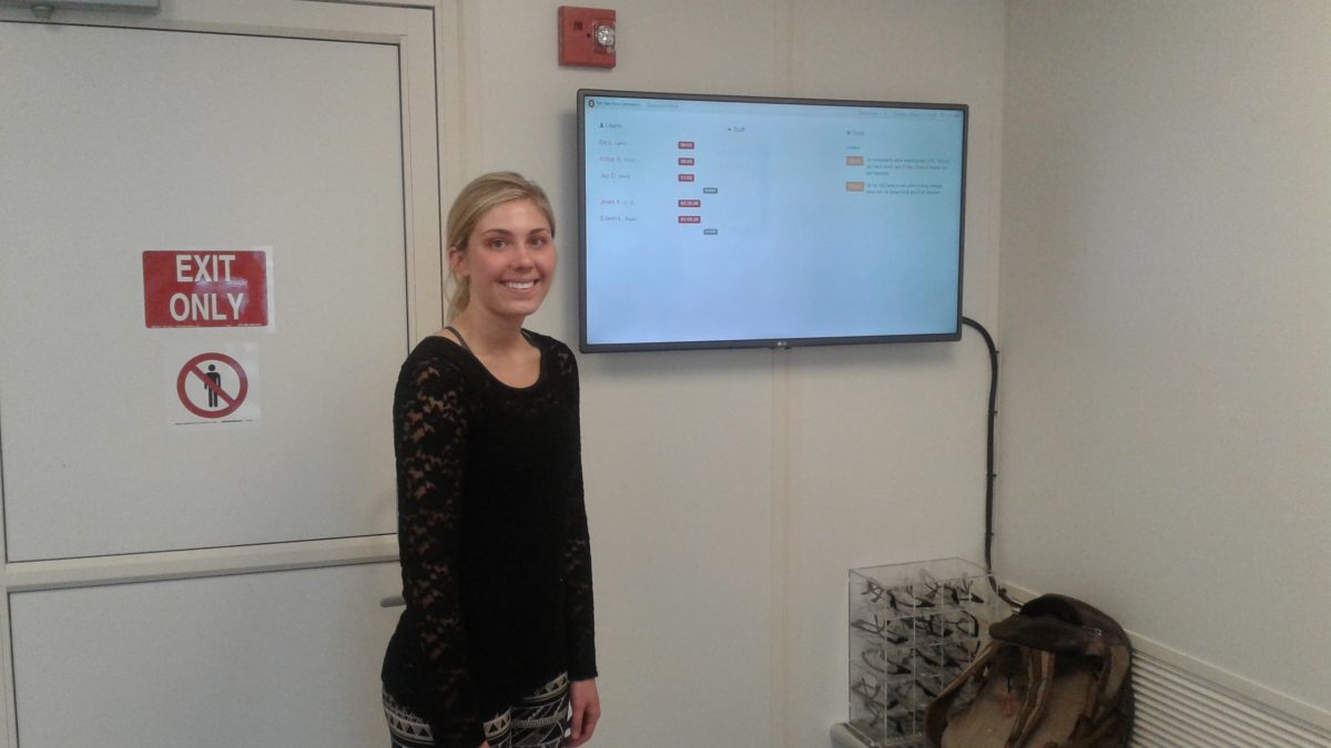
Nanotech West Adds Information Display
A new, large flat panel display is now located in the pre-togging room of the Nanotech West cleanroom. The display continuously pulls information from the NTW central databases and displays information on who is currently in the lab, what tools they are using, and what tools are down or partially operational and their status. In the future it will also …
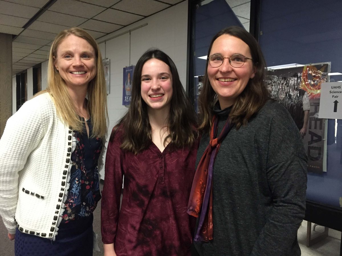
Nanotech West Staff Member Judges UA HS Science Fair
Nanotech West staff member (and IMR Member of the Technical Staff) Aimee Price (L) was a judge in the Upper Arlington High School Science Fair last week. In judging, she happened to run into Prof. Wendy Panero (R), whose daughter, Karen Snyder (Center), was presenting her work on “The Association Between Local Weather and Influenza Hospitalization in Emerging Infections States”. …