 Just about a year ago, we installed a GCA 6100 stepper into the photolithography area of our cleanroom. The stepper complements very nicely the capabilities of the contact aligners and our Vistec EBPG5000 direct-write electron beam lithography tool. The contact aligners are capable of exposing features as big as your substrate consistently across the wafer in a few seconds, but achieving features below ~2.0 microns is difficult. The e-beam is designed to resolve nanometer size features with great placement precision, but it can take hours to write a pattern. The stepper fits in the middle of these two sets of tools; it can print features that are 10′s of millimeters to ~0.60ums in a few seconds per die, or a couple of minutes per wafer, with automated alignment. Additionally, it gives much straighter resist sidewalls than the aligners. Note that in a modern semiconductor fab (factory), a stepper – or yet an even more advanced variety, a “scanner” – is the most commonly used photolithography exposure tool.
 In a contact aligner, a mask is physically placed in contact with the resist on your substrate, and UV light is then blanket exposed through the mask. The only “knob” that you can really control is the exposure time, and you have to look optically through the mask to manually align to previous pattern levels. Our EV620 aligners are broadband tools meaning there are three wavelengths of light used in the exposure: 365nm, 405nm, and 436nm, also known as the “g-line”, “h-line”, and “i-line” of mercury, respectively. Mask damage and wear is yet another issue in the use of contact aligners, especially in production as opposed to research and development (R&D).
 In contrast to the aligner, the stepper setup has a mask , usually referred to as a reticle, that never physically contacts your photoresist-coated wafer. The reticle sits close to the light source, and the UV light is projected through the reticle followed by a 5x reduction lens. One exposure creates one “die”. The wafer sits on an automated x-y stage that “steps” and repeats the single die exposures into an array. You can control both the exposure time and the focus of the UV light. Since the objectives are fixed, previous layers are aligned to the video system based on knowledge of the offset of the alignment keys from the center of the reticle. Our GCA stepper uses only the i-line (365 nm) of the lamp for the exposure, which also somewhat simplifies the photolithography process as well as process transfer from other tools. The 5x reduction also means that features on the reticle can be easier to fabricate, and that any line edge roughness on features on the reticle are reduced by 5x on the final exposed pattern.
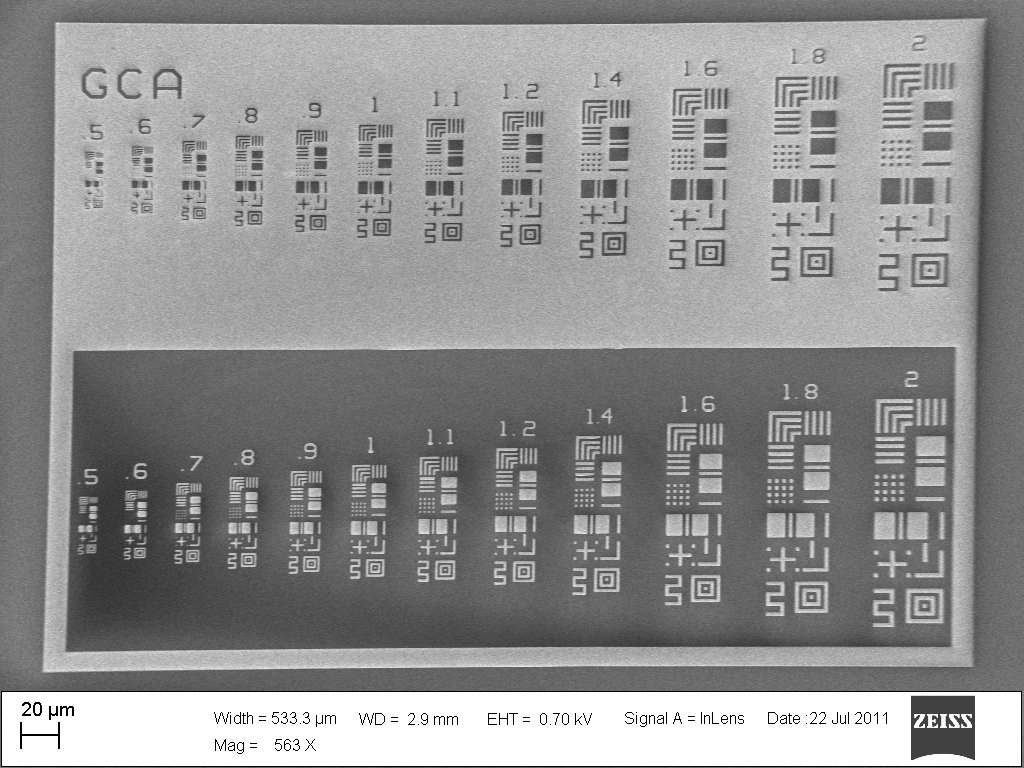
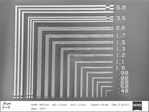
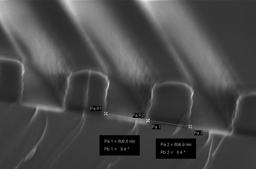
For those of you struggling to get 1.0um features using the aligners, take a look the SEMs below. One micron features, both lines and spaces, should be rather trivial on an i-line stepper of this type that is working properly and has proper focus. In fact, as time and experience progress and as users create new designs, we expect STP01 to be our regular “go-to” photolithography exposure tool even if fine features aren’t needed.
For discussions and/or training on the stepper (STP01) feel free to email me. Nanotech West would once again like to acknowledge the Sensors Directorate of the Wright-Patterson Air Force Base of Dayton, OH for the donation of this tool.
Derek Ditmer
Nanotech West Staff
ditmer.2@osu.edu