Scientists at The Ohio State University earned another key tool for semiconductor research, which is paving the way for advanced technologies beneficial to society.
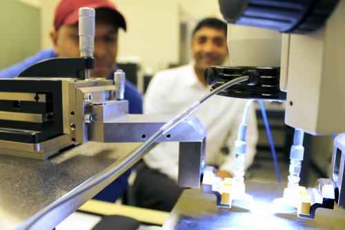
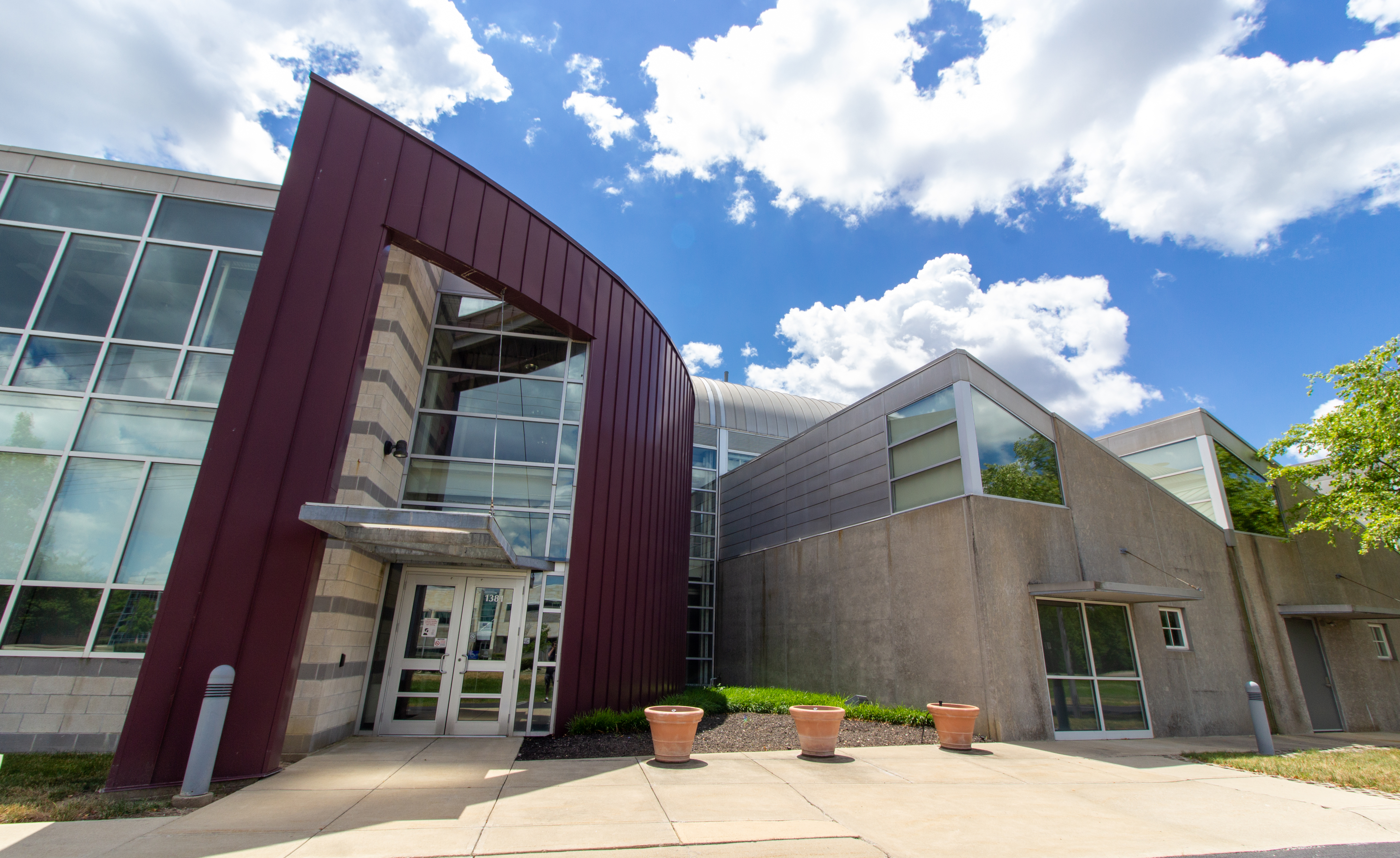
The National Science Foundation approved a $1.5 million Major Research Instrumentation (MRI) toward the purchase and installation of an electron-beam lithography system at Nanotech West Laboratory, operated by the Institute for Materials and Manufacturing Research (IMR).
Principal Investigator Siddharth Rajan, Ohio State professor of Electrical and Computer Engineering (ECE) and Materials Science and Engineering departments, said the system is due for installation by the summer of 2021.
“It will be a highly capable, fast, and user-friendly system, and I look forward to all the great research this new tool will enable,” Rajan said.
Electron beam lithography is a core capability for nanotechnology, and uses a focused beam of electrons to create patterns. This enables researchers to investigate phenomena or design structures with exquisite precision and accuracy at the nanometer scale, which light-based photolithography cannot achieve.
“The ability to create patterns precisely and accurately at the nanometer scale is a key enabler for advancements in science, engineering, and medicine,” Rajan said.
The team involved in the NSF proposal includes co-investigator John Carlin, research scientist and director of the Nanotech West Lab facility, located on Kinnear Road. Other key members include Ohio State Senior Research Associate-Engineer Aimee Price.
The new tool is expected to increase accessibility to lithography capabilities to a broad range of researchers, Price said.
 “As an open-use facility, Nanotech West Lab serves a wide-ranging mix of users from Ohio State and from across the state and region. We want to continue to lead in lithography capabilities and keep pushing forward, past the current limitations in fabrication,” she said. “This system will make training easy and, in turn, allow more of our users to become hands-on in the lab.”
Rajan said better understanding of materials at the nanometer scale can lead to greater societal impact and disruptive innovations. One of the key reasons NSF funded the proposal was the wide-ranging research at Ohio State to benefit from this tool, including next-generation high data rate communication systems; imaging for medical, security, and space remote-sensing applications; quantum information systems; cell engineering for medical applications; and new semiconductor materials for energy-efficient power electronics and computing.
Earlier this year, Nanotech West installed an advanced maskless aligner system, the MLA150 from Heidelberg Instruments. The photolithography system is ideal for rapid prototyping due to its ease of use, high-speed performance and non-contact exposure.
Price said she expects the new electron-beam lithography system funded by NSF will continue to widen the range of Nanotech West’s user capabilities, from contact aligners to e-beam lithography and direct laser-writer tools.
As with all NSF research proposals, a key goal of this project is to increase outreach and to create unique educational opportunities beyond the research community.
ECE Professor Betty Lise Anderson helped spearhead the outreach program aspect of the proposal to further engage students and teachers from schools in the Columbus metropolitan region with scientific research. High school students will learn how fundamental science concepts in waves, optics and electronics connect to real-life applications through hands-on projects and tours of clean room facilities at Ohio State.
Story by Ryan Horns (Communications Specialist | horns.1@osu.edu) with Nanotech West information provided by Mike Huson (IMR Public Relations| huson.4@osu.edu)
Reposted with permission from imr.osu.edu/nsf-funds-1-5m-tool-to-advance-next-gen-nanotechnology-at-nanotech-west-lab/
