
This Nanotech West Lab Research News article was contributed by the group of Prof. Wu Lu, Professor of Electrical and Computer Engineering, of The Ohio State University
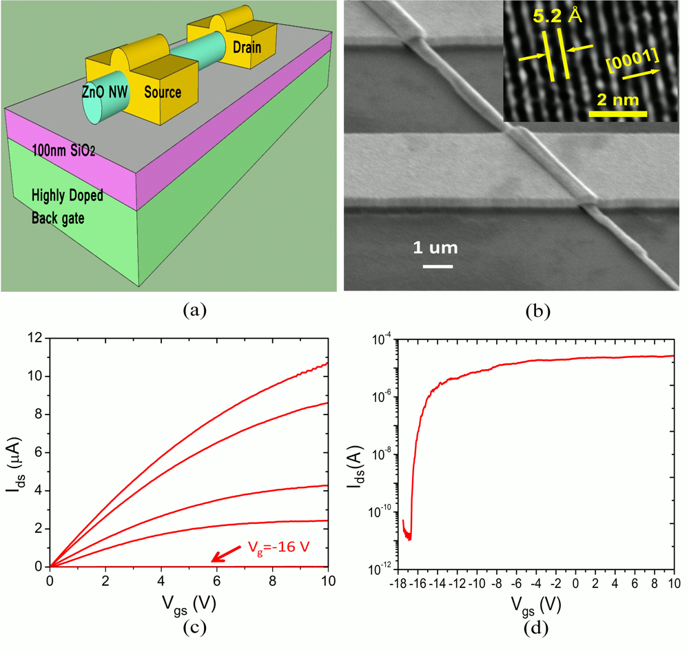
Figure 1: (a) Schematic view of ZnO NW FETs. (b) SEM image
ZnO nanowires (NWs) have attracted great attention as an important material for electronic and optoelectronic device applications due to its wide band gap and high exciton binding energy. It is a native n-type material and the electronic conduction in nominally un-doped ZnO materials is a result from native defects such as unintentionally-doped impurities and structural imperfections. However, owing to its complexity, the electrical transport in ZnO devices is often thought to be controversial. It can be even more intangible in the case of quasi-one-dimensional ZnO NWs based devices. For example, Does the electron transport of ZnO NW field effect transistors (FETs) follow the same mechanism of ZnO thin film FETs? Do they follow the same electron transport mechanism at different temperatures? What is the carrier mobility and trap density in ZnO NW FETs? In addition, electrical contacts on such ZnO NWs are also difficult to characterize due to the lacking of an established model. Because of the high surface to volume ratio of NWs, the hypothesis that metal contacts on ZnO NWs exhibit the same or similar characteristics with those contacts on ZnO thin films is not necessarily true because the Fermi-level can be pinned by surface states. Therefore it is fundamentally important to establish a model and revisit this issue.
In this research, we investigate the electron transport study of ZnO NWs FETs. Our results show that the electron transport of ZnO NW FETs is governed by the space charge limited model at temperatures below a trap temperature. Above the trap temperature, the electron transport is thermionic emission dominated. Based on the space charge limited model, an accurate method is developed for field effect mobility extraction. The extracted electron carrier mobility is strongly dependent on temperature with a peak value of 51 cm2/Vs at 167 K. Under the space-charge limited transport, the field mobility is lower in comparison with the values extracted from the thermionic emission model. The electron mobility due to space charge scattering has a value of 483 cm2/Vs at the trap temperature with temperature dependence of T4∼5. Our results also show that three metal contacts (Al, Au, Ti) are all Schottky contacts to ZnO NWs due to surface states. The surface states related Schottky barrier height (SBH) can be extracted based on a back to back Schottky diodes model and the values are in the range of 0.34–0.37 eV for three metal contacts. The activation energy of these surface states can be determined from the Arrhenius plots, which is in the range of 0.23–0.29 eV. Based on the space-charge-limited model, the surface state density of ZnO NW is in the range of 1.04×10¹⁰–1.24×10¹⁰/cm2.
Fig. 1(a) shows a 3-D schematic view of ZnO NW FETs. The ZnO NW FETs studied here have a back gate design for modulation of current flowing through NWs between source and drain Schottky contacts. Both the scanning electron micrograph and transmission electron micrograph of a fabricated ZnO NW FET are shown in Fig. 1(b). As a working device, a single NW needs to be in good contact with two electrodes. The diameter of the ZnO NWs is 100 nm. The native impurity concentration of ZnO NWs is estimated to be at the level of 1017/cm3. Fig. 1(c) and (d) shows the family Ids–Vds and Ids–Vgs transfer characteristics of a typical Ti/Au contact ZnO NW FET at room temperature, respectively. From the gate modulation of the device one can observe that this is an n-channel depletion mode device with a threshold voltage around −17 V. The device exhibited an excellent current ON/OFF ratio of 106. Au and Al/Au contact devices also exhibited similar transfer characteristics with a similar ON/OFF current ratio.
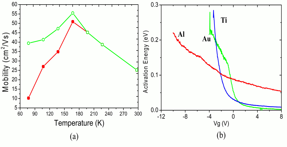
Figure 2: (a) Extracted carrier mobility (b) Activation energy extracted
Fig. 2(a) shows the extracted field mobility as a function of temperature. Starting from 77 K, the mobility increases upon heating until it reaches the maximum value of 51 cm2/Vs at 167 K, which is very close to the trap temperature we extracted (red line). This is likely due to that the scattering between electrons and space charges is dominant as a result of the electron hoping process and the slow motion of electrons at low temperatures. Above the trap temperature, however, electron transport mechanism is no longer space charge dominant and the electron space charge scattering gets negligible. For comparison, the mobility values below the trap temperature extracted using thermionic emission model are also shown in Fig. 2 (a) (in green). Clearly, the conventional method for thin film planar FETs (in green) over-estimates the low field carrier mobility and results in relatively higher values below the trap temperature. Fig. 2(b) shows the extracted activation energy values for Ti/Au, Au, and Al/Au ZnO NW SB-FETs are of 0.29 eV (Ti), 0.28 eV (Au) and 0.23 eV (Al), respectively. These values are close to the oxygen vacancy value reported and also have a good consistence with the extracted Schottky barrier height, suggesting that oxygen vacancies are the major defect levels in these ZnO NWs.
Our results presented here reveal that NW based field effect devices, due to the unique geometric characteristics, may exhibit different electron transport properties at different bias and temperature conditions. Specifically traps like oxygen vacancies and surface and interface states play a critical role on the carrier transport and device performance. Though the model and method developed here are based on ZnO NW SB-FETs, it is worthy to point out that the approach presented here is applicable to other one dimensional semiconductor NW FETs such as carbon nanotubes, Si, Ge, and GaN nanowires. This approach can be a powerful method to study the effects of surface and interface traps and charges and surface passivation on field effect mobility in NW FET devices.
Publications:
Ye Shao,
Jongwon Yoon, Hyeongnam Kim, Takhee Lee, and Wu Lu, “Temperature Dependence of Electron Transport
in ZnO Nanowire Field Effect Transistors,”
IEEE TRANSACTIONS ON ELECTRON DEVICES, vol. 61, pp. 625-630, 2014.
Ye Shao,
Jongwon Yoon, Hyeongnam Kim, Takhee Lee, Wu Lu, “Analysis of surface states in
ZnO nanowire field effect transistors,”
Applied Surface Science, vol 301, pp. 2-8, 2014.
Contact:
Wu Lu, Professor,
Department of Electrical and Computer Engineering, The Ohio State University. Email: lu.173@osu.edu
Acknowledgement:
This research is a collaborative work with Prof. Taehee Lee at Seoul National University.