

This Nanotech West Lab Research News article was contributed by Dr. Santino Carnevale in the research group of Prof. Steven Ringel, Neal A. Smith Chair Professor Electrical and Computer Engineering, of The Ohio State University.
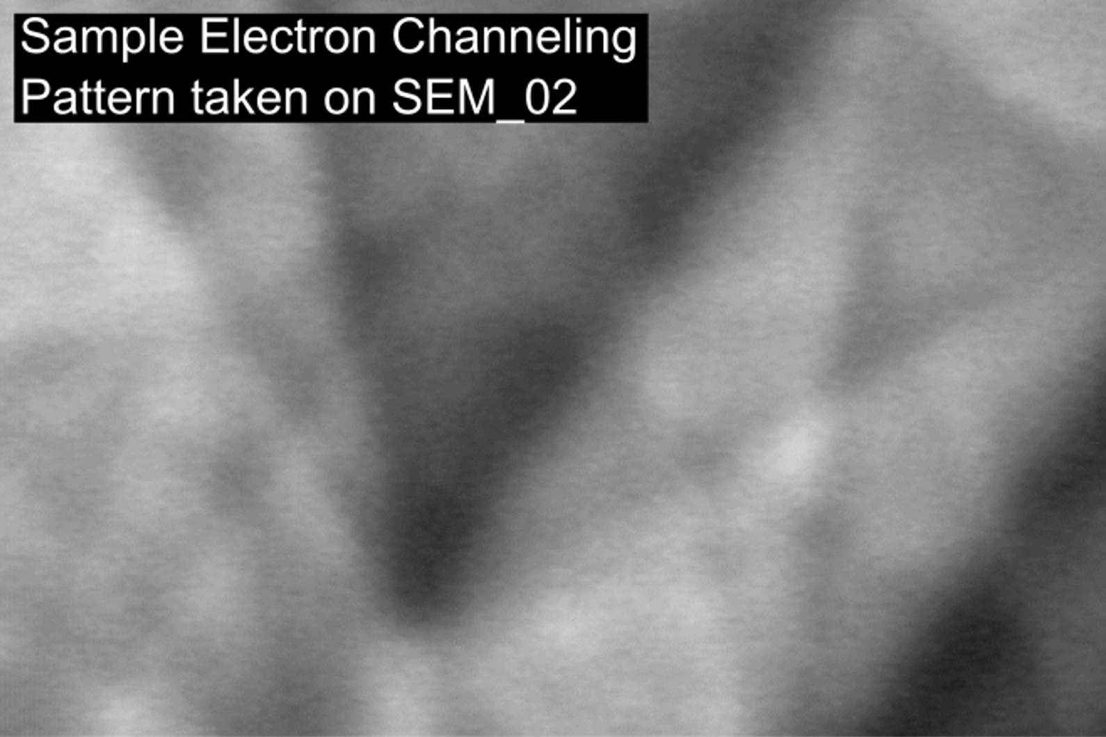
Figure 1: Sample Electron Channeling Patter take on SEM 02
When researchers consider how to image extended defects (e.g. dislocations, stacking faults) in single crystal samples, in all likelihood the first technique they consider is transmission electron microscopy (TEM). After all, TEM has been the most widely used method for characterizing extended defects for decades, and can provide a wealth of information regarding a sample’s microstructure. Unfortunately, TEM imaging requires that samples are electron transparent, which usually means the material needs to be thinned with some combination of polishing and/or focused ion beam milling. This sample preparation can be quite time consuming and possibly lead to a bottleneck in research progress when characterizing a large number of samples.
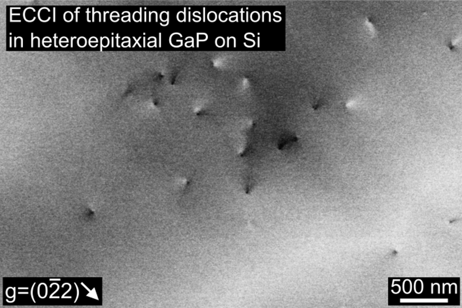
Figure 2: Electron Channeling Contrast Imaging
Here, we discuss our recent efforts to develop/implement a little-known technique called electron channeling contrast imaging (ECCI) that shares many similarities with TEM but requires little to no sample preparation. ECCI is performed in a scanning electron microscope (SEM) equipped with a standard back-scattered electron (BSE) detector. When imaging a single crystal under low magnification with a BSE detector, features called electron channeling patterns (ECPs) become apparent. These features resemble Kikuchi lines found in TEM, and like Kikuchi lines, different areas of an ECP correspond to different diffraction conditions. Thus, it is possible to image with electrons that meet a specific diffraction condition by positioning the optic axis of the SEM so that it coincides with a specific area of an ECP. When imaging with electrons that meet a specific diffraction condition, extended defects exhibit strong contrast because of the deviations from the bulk lattice they create. This is the essence of how ECCI works. In applying ECCI to various semiconductor material systems we have successfully imaged a variety of extended defects, including threading dislocations, misfit dislocations, and stacking faults, in a variety of materials, including GaN, GaP/Si, and GaAsP. Perhaps most importantly, because the electrons that form an ECCI micrograph are backscattered from material near the surface of the sample, no sample thinning is necessary, thus greatly reducing the amount of time needed to characterize a sample compared to TEM.
Examples of an ECP and ECCI image taken at Nanotech West on SEM_02 are provided. The ECP was taken at low magnifications using the back-scattered electron detector when imaging a sample of heteroepitaxial GaP on Si. The ECCI image shows threading dislocations that penetrate the surface of a 1 µm thick layer of GaP/Si sample
S.D. Carnevale, J.I. Deitz, J.A. Carlin, Y.N. Picard, M. De Graef, S.A. Ringel, T.J. Grassman, “Rapid misfit dislocation characterization in heteroepitaxial III-V/Si thin films by electron channeling contrast imaging,” Applied Physics Letters, vol. 104, pp. 232111, Jun. 2014.
S.D. Carnevale, J.I. Deitz, J.A. Carlin, Y.N. Picard, M. De Graef, S.A. Ringel, T.J. Grassman, “Rapid Characterization of Extended Defects in III-V/Si by Electron Channeling Contrast Imaging,” in Photovoltaic Specialist Conference (PVSC), 2014 IEEE 40th, 2014, pp. 2800-2803.