[This Nanotech West Lab Research News article was contributed by the group of Prof. Ron Reano, Associate Professor of Electrical and Computer Engineering, and ElectroScience Laboratory, of The Ohio State University]

Fig. 1. (a) Diagram of the cantilever coupler. In the diagram, the top cladding is made to be transparent in order to make visible the embedded inverse width tapered silicon waveguide. Light from a tapered optical fiber is coupled into a 450 nm by 250 nm cross-section silicon strip waveguide via the cantilever coupler. (b) Main: Top-down SEM image of a fabricated cantilever coupler; Inset: angled view SEM image of the cantilever coupler showing that the coupler is fully released from the substrate.
Silicon photonics is a promising approach for chip-scale integrated optics. A single-mode silicon strip waveguide designed for operation in the infrared, for example, has a typical submicron cross-section of 450 nm x 250 nm. Highly confined optical modes allow for high density integration and waveguide bends with micrometer scale radii of curvature. The high confinement, however, also produces major challenges when attempting to efficiently couple light between silicon strip waveguides and optical fibers. Mode conversion from a single-mode fiber, with mode field diameter equal to 10 micrometers, results in a coupling loss that is greater than 20 dB. Current methods designed to achieve efficient fiber-to-chip coupling generally involve edge coupling using inverse width tapered waveguides or surface coupling using grating couplers. Inverse width tapers enable low loss and broadband edge coupling but require dicing or cleaving the chip. Alternatively, grating couplers enable light coupling via the surface of the chip without the need for cleaving. They require, however, a tradeoff between bandwidth and efficiency.
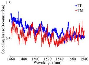
In this research, we present cantilever couplers for fiber-to-chip and chip-to-chip light coupling. Cantilever couplers enable broadband and low loss light coupling to photonic integrated circuits on an entire chip surface without the need for dicing or cleaving the chip. Measurements of fabricated devices demonstrate average coupling losses of 0.62 dB per connection for the TE mode and 0.50 dB per connection for the TM mode across the optical telecommunications C band (1530 nm – 1565 nm) using a silicon inverse width taper length of only 6.5 μm. To the best of our knowledge, this is the shortest fiber-to-strip waveguide coupler employing inverse width silicon tapers reported in the literature.

Fig. 2. Measured coupling loss versus wavelength. The average measured coupling loss values in the optical telecommunications C band are 0.62 dB per connection for the quasi-TE mode and 0.50 dB per connection for the quasi-TM mode.
Figures 1a and 1b show a diagram of the coupling scheme and a scanning electron microscope image of a fabricated coupler, respectively. The cantilever coupler consists of a silicon inverse width tapered strip waveguide embedded within a patterned oxide thin film bilayer cladding. The bilayer cladding consists of plasma enhanced chemical vapor deposition (PECVD) silicon dioxide and buried oxide (BOX). Robust and efficient optical mode conversion between a butt coupled tapered optical fiber and the 450 nm by 250 nm silicon strip waveguide is enabled by both the silicon inverse width taper and the localization provided by the oxide cladding which functions as a micro-fiber. Coupling and propagation losses of fabricated devices are measured in the laboratory by measuring the insertion loss of back-to-back cantilever couplers with interconnecting waveguides with lengths between 250 μm and 2 mm. The measured coupling loss versus wavelength is shown in Fig. 2. Measured coupling losses are less than 1 dB per connection from 1477 nm to 1580 nm.
Publications:
1. P. Sun and R. M. Reano, “Cantilever coupler for intra-chip coupling to silicon photonic integrated circuits,” Opt. Express 17, 4565-4574 (2009).
2. Michael Wood, Peng Sun, and Ronald M. Reano, “Compact cantilever couplers for low-loss fiber coupling to silicon photonic integrated circuits,” Opt. Express 20, 164-172 (2012).
Contact:
Ronald M. Reano, Associate Professor, email: reano.1@osu.edu
Acknowledgement:
This work was supported by the National Science Foundation (NSF).

